[Note: This is a guide to expand a Commodore 610 machine to 1 MB of memory internally. It is a translation of the article in "Heute schon geust?!" number zero with the corrections from "Heute schon geust?!" number 1 already applied. Because bank 15 is still used as system bank after the expansion, 960 kilobyte of memory are available, but BASIC will use only two or four banks (with the BASIC from the Commodore 620/720). Enjoy.]
You might know that the CBM 610/710 has been designed for 256 K RAM on the motherboard. Those thitherto unknowing may be told that for an expansion assembly of U 29 to U 36 and U 45 to U 52 or U 64 to U 79 resp. plus condensators C 66 to C 94 is necessary.
BEWARE MOS! First assemble all condensators, then pin 8, then pin 16, followed by all other pins.
Once finished, bank 1 to 4 are available. BASIC 128 doesn't realize the new memory size while the operating system does. Remedy is the BASIC from the 720.
But today, everybody expects 1 MB memory or address space respectively from a reasonably modern computer. Especially if the used processor is able to manage this space.
For the less deserving, it may be explained here, how dynamic memory is controlled.
The memory cells of a DRAM are ordered in rows and columns like a matrix. At first, the RAM gets the row address together with the signal RAS, whichs flags the validity. This part of the address is remembered by the RAM. After that, the column address is supplied over the same address lines together with the signal CAS. So the 16 address signals necessary for 64 k memory, are actually supplied in two portions of 8. Splitting the addresses into two halves is done in the 610 to 710 by the multiplexers U 92 to U 95.
[Skipped some germanisms here] To address a 256 k memory chip, we need 18 address lines in two portions of 9. For this we will use the address extension lines BP0 and BP1 (A16 and A17) plus an additional multiplexer, a 68 ohm resistor and voila: the additional address line is available for connection to pin 1 of the memory chips.
The PAL (a 82S100) has the job to select the 4 existing memory banks by generating the RAS and CAS signals described above. Why they choose this chip is a good question. Either the thing was available on bargain offer (at Völkner?) or PAL was mistaken for "Pay Additional Luxury". The slowest version of a 20 (instead of 28) pin PAL 16L8 accomplishes the same job in 2/3 of the time for 1/3 of the price.
Use of a coprocessor might make replacement of the PAL advisable, since it has a maximum delay time of 50(!) ns which is quite a penalty for the memory access time (how about the word "memory access time reduction" [this and the preceeding are single words in the german article]).
The PAL decodes the memory banks in the original wiring by the following pattern:
| Bank | BP3 | BP2 | BP1 | BP0 | |
|---|---|---|---|---|---|
| 1 | 0 | 0 | 0 | 1 | (4-7) |
| 2 | 0 | 0 | 1 | 0 | (8-11) |
| 3 | 0 | 0 | 1 | 1 | (12-15) |
| 4 | 0 | 1 | 0 | 0 | (0-3) |
Each new 256 k bank contains sort of 4 banks of 64 k. Both lower address extension signals BP0 and BP1 are already in use in the old circuit for the selection of 64 k banks. So we have to supply the signals BP2 and BP3 to the PAL for decoding instead of BP0 and BP1. The PAL input BP3 must be connected to ground. It will be used later for disabling the DRAM.
To access all four 256 k banks, a 1 is needed at PAL input BP2. It is generated by combining the signals BP2 and BP3 using a nor gate. A simpler solution, which saves two wire connections is possible, but as a consequence the memory layout becomes so confusing that trouble shooting is a nuisance.
It may be pointed out that the operating system detects available memory from bank 1 to bank 14. Mirrored RAM will confuse the operating system and will impact proper functioning. For this reason, and because additional decoding leads to an unnecessary hay wire circuit, I plead for a full extension to 1 Mbyte.
[Lots of (for me) untranslatable german jokes removed in this section]
After the hopefully pleasuring preliminary memory test, we're about to tackle the remaining ICs and condensators.
When assembling tantal condensators, pay attention to the polarity.
A MOS compliant solder iron is required.
With regard to a future use of a coprocessor, 120 ns memory chips should be used.
Parts list:
| 32 | 41256-120 or similar |
| 32 | tantal or ceramic condensators 100 nF, 5.08 mm wire spacing |
| 1 | resistor 68 ohm |
| 1 | 74S153 |
[That's it. The article mentions help from the club, but since the club doesn't exist any longer, you're on your own. You might draw hope from the fact that I successfully upgraded my machine using above guide.]
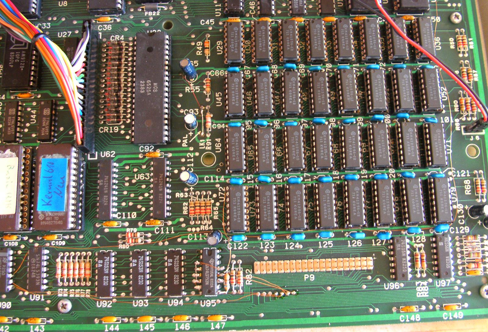
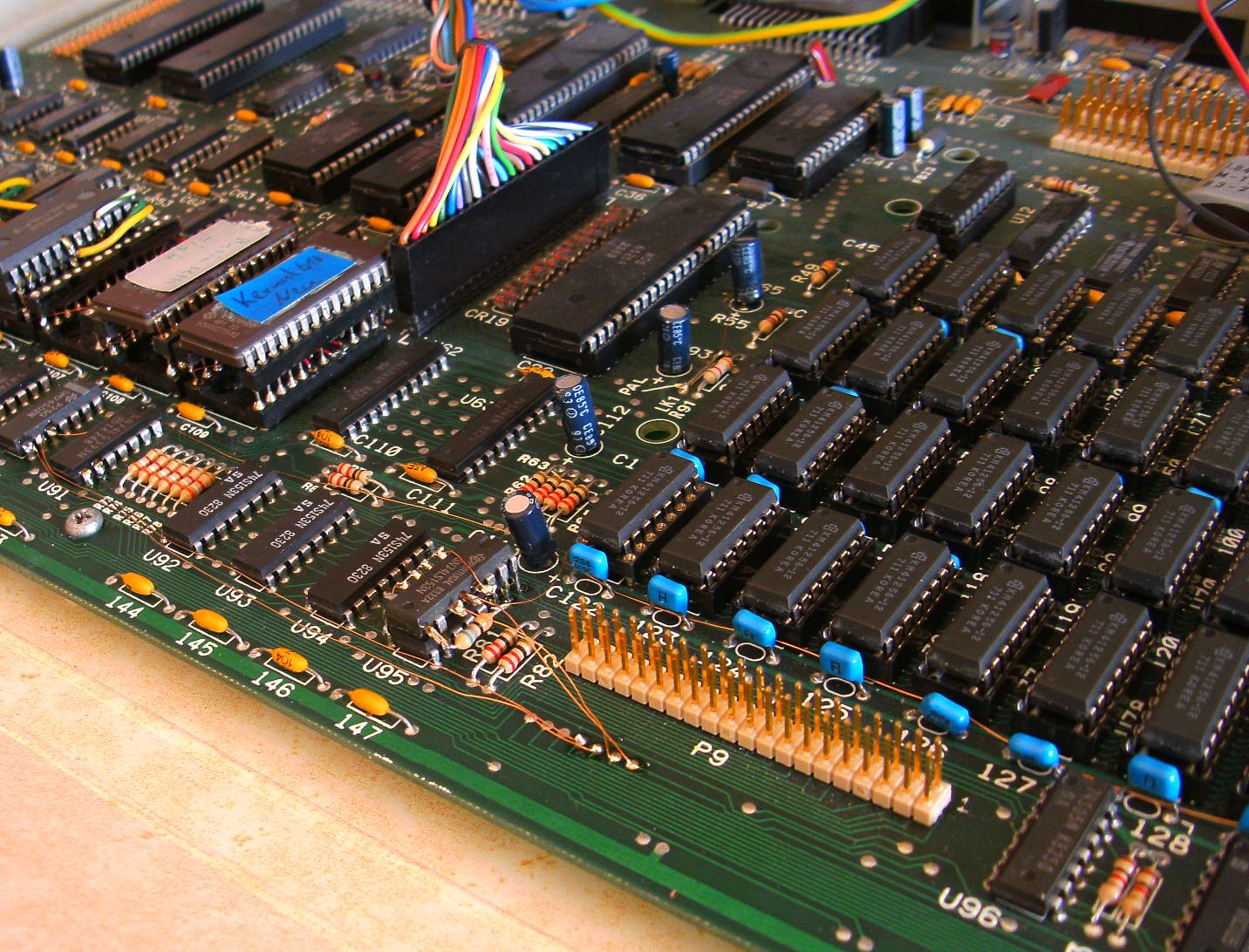
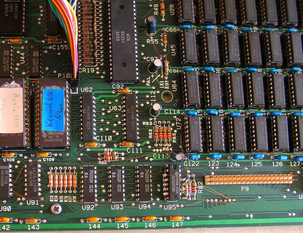
A few photos from my machine that has the memory expansion:
|
|
|
Click on the photos for larger versions.
There's an article in HSG1 on how to map part of the expanded memory into the system bank. I might come up with a translation later.]
![]()
| memory-expansion.php Letzte Änderung: 04-Apr-2015 | Impressum Datenschutzerklärung |